The principle of operation will be explained using a gedanken experiment, an experiment, which is in principle possible but not necessarily executable in practice. We imagine that one can bring both semiconductor regions together, aligning both the conduction and valence band energies of each region. This yields the so-called flatband diagram shown in Figure below
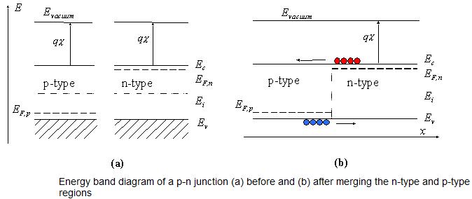 Note that this does not automatically align the Fermi energies, EF,n and EF,p. Also, note that this flatband diagram is not an equilibrium diagram since both electrons and holes can lower their energy by crossing the junction. A motion of electrons and holes is therefore expected before thermal equilibrium is obtained. The diagram shown in Figure above (b) is called a flatband diagram. This name refers to the horizontal band edges. It also implies that there is no field and no net charge in the semiconductor.
Wednesday, June 9, 2010
Flatband diagram of pn Junctions
Posted by Unknown on Wednesday, June 09, 2010


0 comments:
Post a Comment